—– 28.224 MHz Continuous Wave Receiver. —–
One of the most interesting and challenging projects that I did at Texas Tech was building a high gain RF receiver. My team was responsible for carrying the project from the specification stage, through the theory and design stages, to a final professionally designed PCB product. This is a brief technical description of the project:
- High gain 28.224 MHz CW Super Heterodyne Receiver designed to pick up Morse code, uses multiple frequency spread amplifiers to converts signals as low as -95dBm to an audible signal.
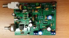
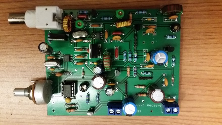
This is a picture of our final product; a green-board PCB design for the 28.224 MHz AM Receiver.
I took responsibility for the planning/theory, and design/prototyping stages for our project.
During the planning and design stages Dr. Michael Helm’s excellent book: Practical Radio Frequency Circuit Design was very helpful for me, and provided an excellent reference for different RF typologies and typical values useful for them.
This is a sketch of the design I used when prototyping:
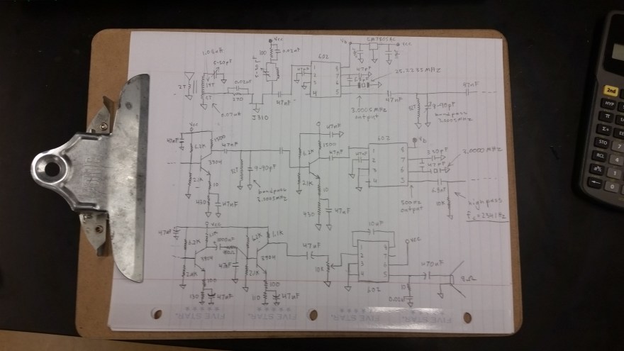
This is the final circuit design created through a combination of theory, circuit simulations, and prototyping:

The receiver is designed to output audible reproductions of Morse Code from a pulsed CW AM signal being transmitted at the weather beacon site. .
The transmitter site puts out a AM RF waveform, and the Morse Code is encoded as a pulsed CW signal. This type of signal scheme is show below:

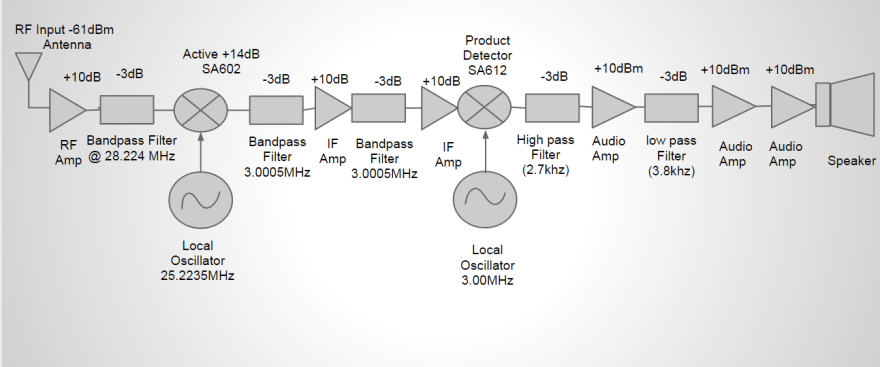
The design uses a Super Heterodyne Receiver typology, which uses frequency spread amplification to reduce the noise or distortion of the signal. The block diagram for the receiver design is show below.
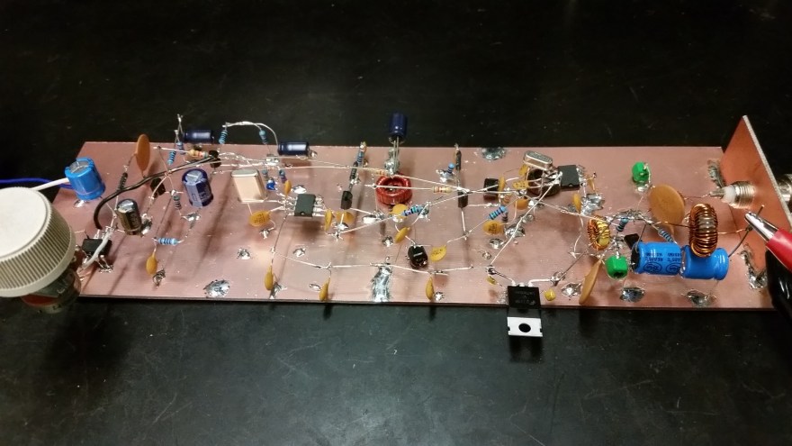
Initial prototyping & testing was done with sky-wiring on a copper clad board.
Video of the working reciver prototyping, being tested with a -95.7dBm RF signal source.
After the final design had been established and thoroughly tested, my team designed a PCB in EAGLE CAD, and sent in the design to be manufactured.
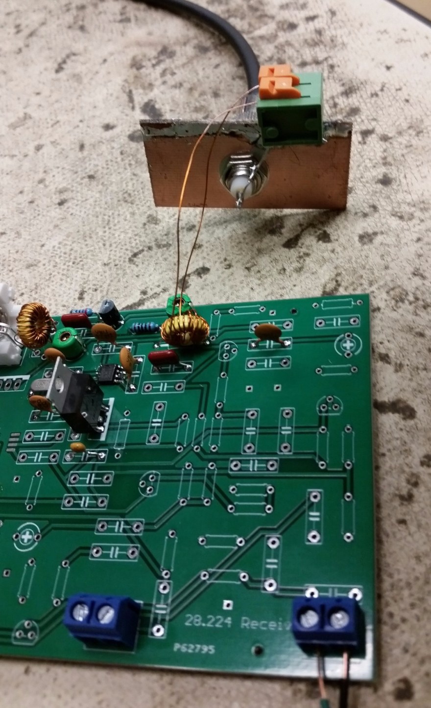
After the PCB arrived we populated and tested it. (we did run into some problems.) Here I am troubleshooting the PCB, at the first stage output filter.
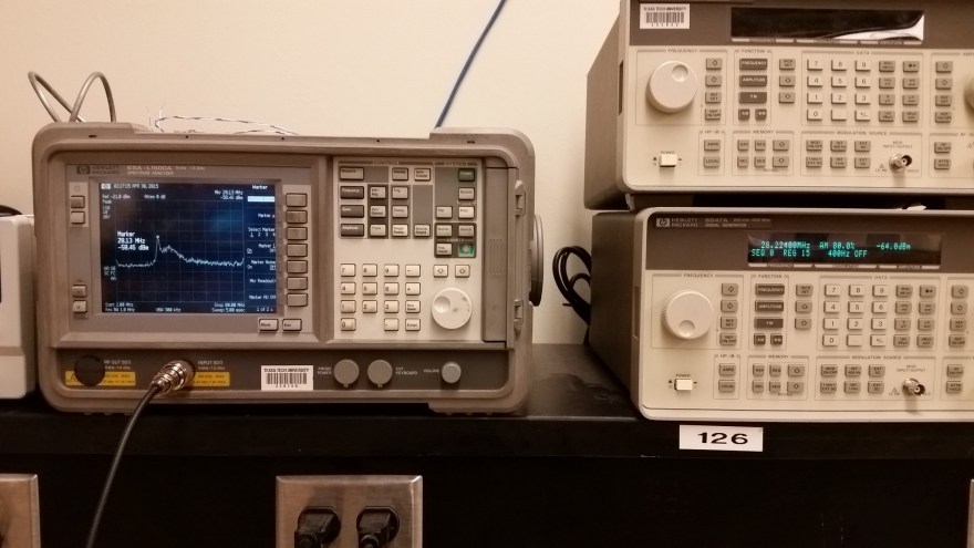
Set up using the spectrum analyzer and a RF signal generator to test the gain at the first stage output filter. It shows a gain of about 15 dBm, from the input signal.
This is a picture of our final product: A green-board PCB design for the 28.224 MHz AM Receiver.
